2023. 1. 26. 19:47ㆍ기록지/컴퓨터구조(computer architecture)
2-to-1, 8-to-1 Mutiplexer 구현
디지털 설계를 위해 기초로 사용할 수 있는 회로를 Verilog로 모델링 한다. 2-to-1, 8-to-1 Multiplexer를 구현해 보고 simulation을 통해 제대로 설계되었는지 검증한다.
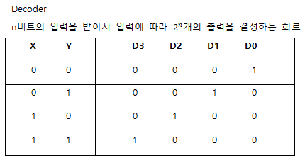
Demultiplexer
멀티플렉서의 역기능을 수행하는 조합 논리회로로써 선택 선을 통해 여러 개의 출력선 중 하나의 출력 선에만 출력을 전달한다.
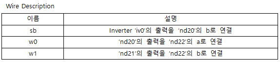
Named mapping
mx2 test_mx2 (.y(tb_y),.d0(tb_d0),.d1(tb_d1),.s(tb_s)); 이와 같이 mx2라는 모듈에서 사용한 wire 와 top level에서 사용하는 wire를 각각 명시해서 연결하는 것을 Named mapping이라한다.
Ordered mapping
_nand2 U1_nand2(tb_a, tb_b, tb_y1); 이처럼 top level에서 선언한 wire만을 사용해서 port map하는 것을 ordered mapping이라고 한다. 앞에서부터 순서대로 연결하는 방식이라서 named 방식에 비해 실수를 유발할 확률이 높다.
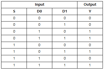
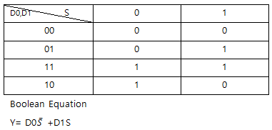
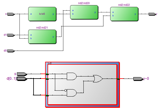
2-to-1 multiplexer 설계 세부사항
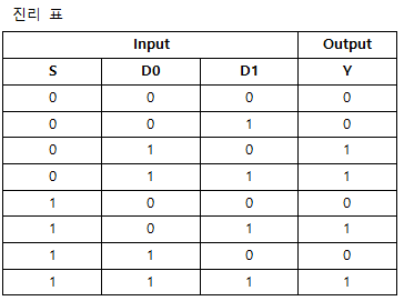
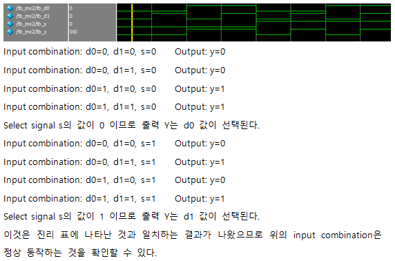
설계 검증
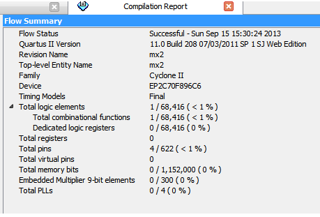
Synthesis 결과
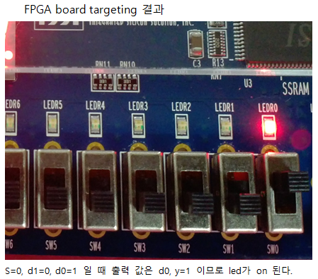
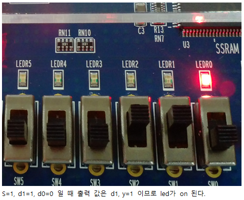
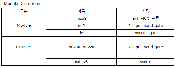
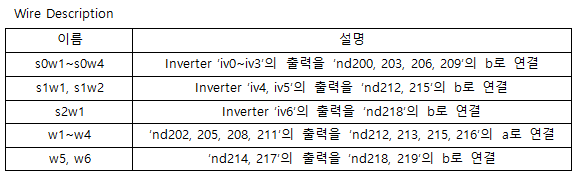
8-to-1 multiplexer 설계 세부사항
설계 검증
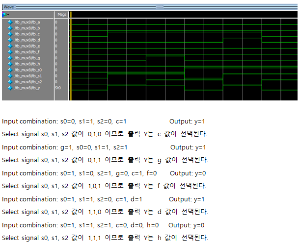
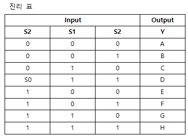
진리 표에 나타난 것과 일치하는 결과가 나왔으므로 위의 input combination은 정상 동작하는 것을 확인할 수 있다.
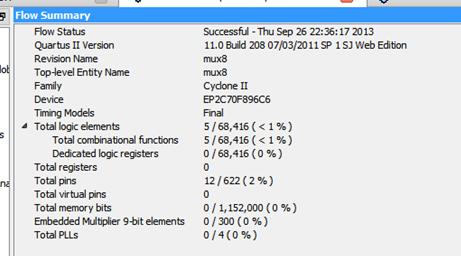
Synthesis 결과
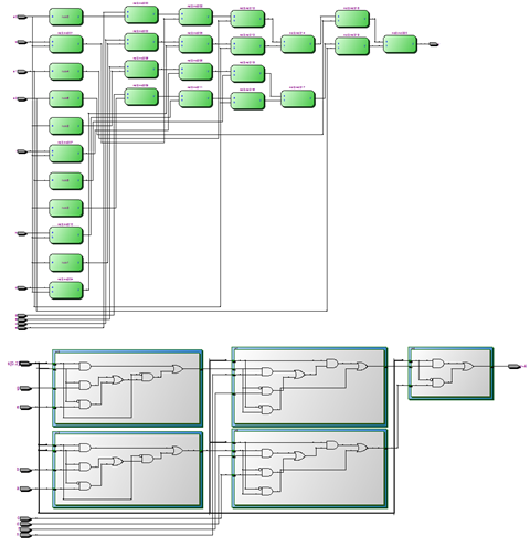
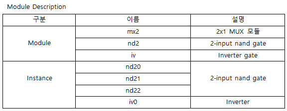
source code (verilog)
2-to-1
module mx2 (y, d0, d1, s);

	input d0, d1, s;
	output y;

	wire w0,w1,sb;

	iv iv0(.a(s),.y(sb));
	nd2 nd20(.a(d0),.b(sb),.y(w0));
	nd2 nd21(.a(d1),.b(s),.y(w1));
	nd2 nd22(.a(w0),.b(w1),.y(y));

endmodule

module iv(a,y);

	input a;
	output y;

	assign y=~a;

endmodule

module nd2(a,b,y);

	input a,b;
	output y;

	assign y=~(a&b);

endmodule


`timescale 1ns/100ps
module tb_mx2;

	reg tb_d0, tb_d1, tb_s;
	wire tb_y;

	mx2 test_mx2 (.y(tb_y),.d0(tb_d0),.d1(tb_d1),.s(tb_s));

	initial

	begin
	tb_s=0; tb_d0=0; tb_d1=0;
	#10; tb_d1=1;
	#10; tb_d0=1;tb_d1=0;
	#10; tb_d1=1;
	#10; tb_s=1; tb_d0=0;tb_d1=0;
	#10; tb_d1=1;
	#10; tb_d0=1;tb_d1=0;
	#10; tb_d1=1;
	#10; $finish;
	end

endmodule
8-to-1
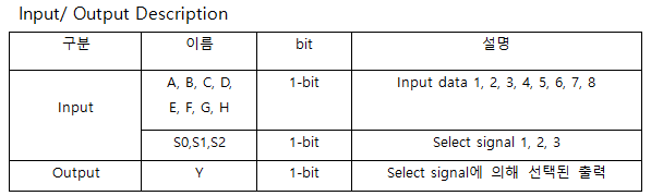
module mux8 (y, a, b, c, d, e, f, g, h, s0, s1, s2); // 8-to-1 multiplexer module

	input a, b, c, d, e, f, g, h, s0, s1, s2;  //input
	output y;  //output

	wire wa,wb,wc,wd,we,wf,wg,wh,wi,wj,wk,wl,wm,wn;     //wire
	wire w1,w2,w3,w4,w5,w6,s0w1,s0w2,s0w3,s0w4,s1w1,s1w2,s2w1;  //wire

		//instance of inverter iv0~iv6
	iv iv0(.a(s0),.y(s0w1));
	iv iv1(.a(s0),.y(s0w2));
	iv iv2(.a(s0),.y(s0w3));
	iv iv3(.a(s0),.y(s0w4));
	iv iv4(.a(s1),.y(s1w1));
	iv iv5(.a(s1),.y(s1w2));
	iv iv6(.a(s2),.y(s2w1));

		//instance of nand nd200~nd220
	nd2 nd200(.a(a),.b(s0w1),.y(wa));
	nd2 nd201(.a(b),.b(s0),.y(wb));
	nd2 nd202(.a(wa),.b(wb),.y(w1));
	nd2 nd203(.a(c),.b(s0w2),.y(wc));
	nd2 nd204(.a(d),.b(s0),.y(wd));
	nd2 nd205(.a(wc),.b(wd),.y(w2));
	nd2 nd206(.a(e),.b(s0w3),.y(we));
	nd2 nd207(.a(f),.b(s0),.y(wf));
	nd2 nd208(.a(we),.b(wf),.y(w3));
	nd2 nd209(.a(g),.b(s0w4),.y(wg));
	nd2 nd210(.a(h),.b(s0),.y(wh));
	nd2 nd211(.a(wg),.b(wh),.y(w4));
	nd2 nd212(.a(w1),.b(s1w1),.y(wi));
	nd2 nd213(.a(w2),.b(s1),.y(wj));
	nd2 nd214(.a(wi),.b(wj),.y(w5));
	nd2 nd215(.a(w3),.b(s1w2),.y(wk));
	nd2 nd216(.a(w4),.b(s1),.y(wl));
	nd2 nd217(.a(wk),.b(wl),.y(w6));
	nd2 nd218(.a(w5),.b(s2w1),.y(wm));
	nd2 nd219(.a(w6),.b(s2),.y(wn));
	nd2 nd220(.a(wm),.b(wn),.y(y));


endmodule

module iv(a,y);  // inverter module

	input a;
	output y;

	assign y=~a;

endmodule

module nd2(a,b,y); // nand module

	input a,b;
	output y;

	assign y=~(a&b);

endmodule

`timescale 1ns/100ps   // unit:1ns , precision:100ps

module tb_mux8;  // test bench mux8

	reg tb_a,tb_b,tb_c,tb_d,tb_e,tb_f,tb_g,tb_h,tb_s0,tb_s1,tb_s2;
	wire tb_y;

	// named port mapping
	mux8 test_mux8(.y(tb_y),.a(tb_a),.b(tb_b),.c(tb_c),.d(tb_d),.e(tb_e),.f(tb_f),.g(tb_g),.h(tb_h),.s0(tb_s0),.s1(tb_s1),.s2(tb_s2));

	initial
	begin
	tb_s0=0;tb_s1=0;tb_s2=0;tb_a=0;tb_b=0;tb_c=0;tb_d=0;tb_e=0;tb_f=0;tb_g=0;tb_h=0;
	#10; tb_s1=1;tb_c=1;     // #10 : delay of 10 time unit
	#10; tb_s2=1;tb_g=1;
	#10; tb_s0=1;tb_s1=0;tb_g=0;
	#10; tb_s1=1;tb_s2=0;tb_d=1;
	#10; tb_s2=1;tb_c=0;tb_d=0;
	#10; $finish;
	end

endmodule'기록지 > 컴퓨터구조(computer architecture)' 카테고리의 다른 글
| Quartus II/ ModelSim을 이용한 구현 - 4. ALU(Arithmetic Logic Unit), Substractor (0) | 2023.01.29 |
|---|---|
| Quartus II/ ModelSim을 이용한 구현 - 3. CLA(Carry Look-ahead Adder) (verilog) (0) | 2023.01.28 |
| Quartus II/ ModelSim을 이용한 구현 - 2. RCA(Ripple-Carry Adder) (verilog) (0) | 2023.01.27 |
| SingleCycleCpu(verilog) 설계검증 (0) | 2022.12.24 |
| SingleCycleCPU(verilog) (1) | 2022.12.24 |